Esta PCB utiliza laminados I-Tera MT40 e prepreg RO4450F (PP), garantindo integridade de sinal superior para aplicações digitais de alta velocidade e RF/micro-ondas. Ela apresenta acabamento de Ouro de Imersão (ENIG) de 2u", máscara de solda verde dupla face com serigrafia branca, e é projetada para atender aos rigorosos requisitos de desempenho de sistemas de alta confiabilidade através de controle dimensional preciso, gerenciamento estrito de impedância e protocolos de qualidade rigorosos.
Detalhes da PCB
| Parâmetro de Construção |
Especificação |
| Material base |
I-Tera MT40 + Prepreg RO4450F |
| Contagem de camadas |
6 camadas |
| Dimensões da placa |
99mm × 99mm por peça |
| Espessura final da placa |
1.501mm (após laminação) |
| Peso final do cobre |
Camadas externas: 2oz; Camadas internas: 1oz de cobre acabado |
| Acabamento superficial |
Ouro de Imersão (ENIG), 2u" |
| Máscara de Solda e Serigrafia |
Dupla face: Máscara de solda verde e serigrafia branca |
| Controle de Impedância |
Camada SUPERIOR: trilha de 5mil, controle de impedância single-ended, 50 ohm |
| Configuração de Vias |
Vias cegas; vias de 0.3mm com preenchimento de resina e cobertura de galvanoplastia para nivelamento |
| Recurso Especial |
Plating de borda (metalização de borda) |
| Teste de qualidade |
Teste elétrico 100% realizado antes do envio |
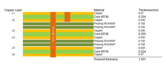
Stack-up da PCB
| Tipo de Camada |
Especificação (de Cima para Baixo) |
| Camada de Cobre (Externa) |
Camada_de_cobre_1 (TOPO): 2oz (70μm) |
| Camada Dielétrica |
I-Tera MT40: 0.254mm |
| Camada de Cobre (Interna) |
Camada_de_cobre_2: 1oz (35μm) |
| Camada de Prepreg (PP) - RO4450F (Camada 1) |
Prepreg RO4450F - 0.102mm |
| Camada de Prepreg (PP) - RO4450F (Camada 2) |
Prepreg RO4450F - 0.102mm |
| Camada de Cobre (Interna) |
Camada_de_cobre_3: 1oz (35μm) |
| Camada de Núcleo |
I-Tera MT40: 0.305mm |
| Camada de Cobre (Interna) |
Camada_de_cobre_4: 1oz (35μm) |
| Camada de Prepreg (PP) - RO4450F (Camada 1) |
Prepreg RO4450F - 0.102mm |
| Camada de Prepreg (PP) - RO4450F (Camada 2) |
Prepreg RO4450F - 0.102mm |
| Camada de Cobre (Interna) |
Camada_de_cobre_5: 1oz (35μm) |
| Camada Dielétrica |
I-Tera MT40: 0.254mm |
| Camada de Cobre (Externa) |
Camada_de_cobre_6 (Inferior): 2oz (70μm) |

Tipo de Arte
Para garantir a fabricação precisa e eficiente da PCB, a arte fornecida para esta PCB está no formato Gerber RS-274-X, que é o formato de arquivo padrão da indústria para fabricação de PCBs.
Padrão de Qualidade
Esta PCB é fabricada e inspecionada em estrita conformidade com o padrão IPC-Classe-2, um padrão amplamente adotado na indústria para placas de circuito impresso. O IPC-Classe-2 especifica requisitos para produtos eletrônicos em geral, garantindo desempenho confiável em aplicações típicas.
Disponibilidade
Esta PCB é oferecida globalmente, com capacidade de fornecimento estável para acomodar diversas necessidades de pedidos — desde protótipos de pequenos lotes até produção em massa em larga escala — apoiada por soluções logísticas eficientes para garantir entrega global pontual.
Introdução ao Material I-Tera MT40
Os materiais laminados I-Tera MT40 estão disponíveis nas formas de laminado e prepreg, em espessuras típicas e tamanhos de painel padrão, fornecendo uma solução completa de material para projetos de circuito impresso multicamadas digitais de alta velocidade, híbridos, RF/micro-ondas, multicamadas e dupla face. Ao contrário dos materiais laminados à base de PTFE, o I-Tera MT40 não requer nenhum tratamento especial de furos passantes, simplificando os processos de fabricação e reduzindo os custos de produção. Ele possui classificação UL 94 V-0, garantindo alta retardância à chama e adequação para uma ampla gama de aplicações eletrônicas. MT40 é um material dielétrico de alto desempenho projetado especificamente para os projetos de circuito impresso digitais de alta velocidade e RF/micro-ondas de hoje. Ele apresenta uma constante dielétrica (Dk) estável em uma ampla faixa de temperatura (-55°C a +125°C) e até frequências de banda W, combinada com um baixo fator de dissipação (Df) de 0.0031, tornando-o uma alternativa econômica ao PTFE e outros materiais laminados comerciais de micro-ondas e digitais de alta velocidade.
Os materiais laminados I-Tera MT40 estão disponíveis nas formas de laminado e prepreg, em espessuras típicas e tamanhos de painel padrão, fornecendo uma solução completa de material para projetos de circuito impresso multicamadas digitais de alta velocidade, híbridos, RF/micro-ondas, multicamadas e dupla face. Ao contrário dos materiais laminados à base de PTFE, o I-Tera MT40 não requer nenhum tratamento especial de furos passantes, simplificando os processos de fabricação e reduzindo os custos de produção. Ele possui classificação UL 94 V-0, garantindo alta retardância à chama e adequação para uma ampla gama de aplicações eletrônicas.O desempenho térmico do I-Tera MT40 é excepcional, com uma temperatura de transição vítrea (Tg) de 215°C (DSC), 230°C (DMA) e 210°C (TMA), e uma temperatura de decomposição (Td) de 360°C com perda de 5% de peso. Isso garante que o material mantenha a estabilidade estrutural e a integridade do desempenho durante ciclos de processamento e operação em alta temperatura, tornando-o ideal para aplicações de alta confiabilidade.
Características do Material I-Tera MT40
Propriedade do Material
| Valor Típico |
Unidades |
Método de Teste |
Temperatura de Transição Vítrea (Tg) por DSC |
| 215 |
°C |
IPC-TM-650 2.4.24.6 |
Temperatura de Transição Vítrea (Tg) por DMA |
| 230 |
°C |
IPC-TM-650 2.4.24.6 |
Temperatura de Transição Vítrea (Tg) por TMA |
| 210 |
°C |
IPC-TM-650 2.4.24.6 |
Condutividade Térmica |
| 360 |
°C |
IPC-TM-650 2.4.24.6 |
Tempo para Delaminação (T260, Cobre removido) |
| >60 |
Minutos |
IPC-TM-650 2.4.24.1 |
CTE no Eixo Z (Pré-Tg) |
| 55 |
ppm/°C |
IPC-TM-650 2.4.24C |
Condutividade Térmica |
| 290 |
ppm/°C |
IPC-TM-650 2.4.24C |
Condutividade Térmica |
| 12 |
ppm/°C |
IPC-TM-650 2.4.24C |
Condutividade Térmica |
| 0.61 |
W/m·K |
ASTM E1952 |
Constante Dielétrica (Dk) @ 2 GHz |
| 3.45 |
— |
Bereskin Stripline |
Fator de Dissipação (Df) @ 2 GHz |
| 0.0031 |
— |
Bereskin Stripline |
Absorção de Umidade |
| 0.1 |
% |
IPC-TM-650 2.6.2.1A |
Inflamabilidade |
| V-0 |
Classificação |
UL 94 |
Aplicações Típicas do I-Tera MT40 |
-Projetos de circuito impresso digitais de alta velocidade
-Sistemas de comunicação RF/micro-ondas
-Projetos de PCB multicamadas e dupla face
-Placas de circuito impresso híbridas
-Equipamentos eletrônicos de alta confiabilidade que exigem desempenho elétrico e térmico estável
-Aplicações de alta frequência sensíveis ao custo (alternativa aos materiais de PTFE)
O que é Controle de Impedância Single-Ended?
O controle de impedância single-ended (também referido como controle de impedância de extremidade única) é um processo crítico de projeto e fabricação de PCB que garante que a impedância característica de uma única trilha condutora na PCB permaneça consistente e corresponda ao valor especificado (neste caso, 50 ohm para a trilha de 5mil na camada SUPERIOR). Impedância é a oposição total ao fluxo de corrente alternada (AC) em um circuito, combinando resistência, capacitância e indutância.
Para aplicações digitais de alta velocidade e RF/micro-ondas, manter uma impedância single-ended precisa é essencial por várias razões: minimiza a reflexão de sinal, reduz a distorção de sinal e o crosstalk, garante a transmissão eficiente de sinal e previne problemas de integridade de sinal que podem degradar o desempenho dos sistemas eletrônicos. A trilha de 5mil na camada SUPERIOR desta PCB é controlada para 50 ohm, que é um valor de impedância padrão para muitas aplicações de RF e digitais de alta velocidade, garantindo compatibilidade com outros componentes e sistemas.
O controle de impedância single-ended é alcançado através do projeto cuidadoso da largura da trilha, espessura da trilha, espessura do material dielétrico e a distância entre a trilha e o plano de referência. Um controle de fabricação rigoroso também é necessário para garantir a consistência nas propriedades do material e nas dimensões da trilha, pois qualquer variação pode alterar o valor da impedância.
Por que o Plating de Borda (Metalização de Borda) é Necessário?
O plating de borda, também conhecido como metalização de borda, é um processo de fabricação de PCB que envolve a metalização das bordas expostas da PCB com um metal condutor (tipicamente cobre, seguido por ENIG para corresponder ao acabamento superficial). Este processo é incorporado ao projeto desta PCB por várias razões importantes, todas as quais aprimoram o desempenho, a confiabilidade e a fabricabilidade da placa:
Melhora do Aterramento e Blindagem: O plating de borda fornece um caminho condutor contínuo ao redor do perímetro da PCB, aprimorando a integridade do aterramento e reduzindo a interferência eletromagnética (EMI). Ele atua como uma gaiola de Faraday, blindando os circuitos internos contra EMI externa e impedindo que sinais internos irradiem para fora, o que é crítico para aplicações de RF e digitais de alta velocidade.
Aprimoramento da Resistência Mecânica: A metalização nas bordas da PCB aumenta a robustez mecânica da placa, tornando-a mais resistente a lascamentos de borda, rachaduras e danos durante o manuseio, montagem e uso operacional. Isso é particularmente importante para PCBs usadas em ambientes hostis ou aplicações com alto estresse mecânico.
Melhora da Dissipação Térmica: O plating de borda serve como um caminho térmico adicional, ajudando a dissipar o calor gerado pelos componentes na PCB. Isso melhora o gerenciamento térmico da placa, prevenindo o acúmulo térmico e garantindo a estabilidade e a longevidade dos componentes eletrônicos.
Facilita a Continuidade Elétrica: O plating de borda pode fornecer continuidade elétrica entre múltiplas camadas da PCB, simplificando o projeto de aterramento e garantindo desempenho elétrico consistente em toda a placa. Ele também ajuda a reduzir a resistência nas bordas da placa, melhorando a integridade do sinal.
Aprimoramento da Soldabilidade e Montagem: O plating de borda fornece uma superfície limpa e condutora que pode facilitar a soldagem de componentes ou conectores montados perto das bordas da placa, melhorando a confiabilidade do processo de montagem.

 Por favor verifique seu email!
 Portuguese